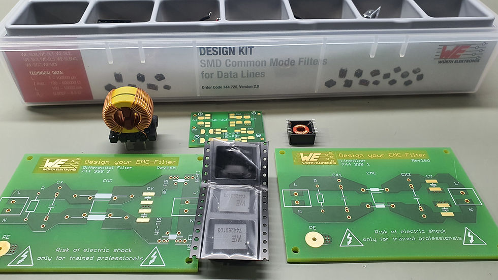
Build-In EMC/EMI HW design
- 25 בפבר׳ 2024
- זמן קריאה 2 דקות
עודכן: 29 בפבר׳ 2024

Electromagnetic Compatibility (EMC) and Electromagnetic Interference (EMI) are crucial considerations in hardware design (HW) to ensure that electronic devices can operate without interference in their intended environment and don't emit harmful interference to other devices. Here's a general outline for building EMC/EMI hardware design:
Design Requirements Analysis:
Understand the regulatory standards and requirements applicable to your product's target markets (e.g., FCC regulations in the US, CE marking requirements in the EU).
Define EMC/EMI specifications and limits for emissions and susceptibility.
PCB Layout and Stackup Design:
Use multilayer PCBs with proper stackup to control impedance and reduce noise coupling.
Separate analog and digital components and signals to minimize interference.
Implement a solid ground plane and use proper power distribution techniques to reduce ground loops and noise.
Place high-speed components and traces carefully to minimize signal reflections and crosstalk.
Component Selection:
Choose components with low EMI emissions and susceptibility.
Use components with built-in EMI suppression features, such as ferrite beads, EMI filters, and shielded connectors.
Grounding and Shielding:
Implement proper grounding techniques, including star grounding and chassis grounding.
Use shielding techniques such as metal enclosures, shields over sensitive components, and shielded cables to contain EMI emissions and protect against external interference.
Filtering and Decoupling:
Incorporate passive components like capacitors and inductors for filtering and decoupling to suppress high-frequency noise.
Place decoupling capacitors close to the power pins of active components to provide local energy storage and reduce voltage fluctuations.
Signal Integrity Analysis:
Perform signal integrity analysis to ensure signal quality and minimize reflections, ringing, and jitter.
Use tools like impedance calculators and simulation software to optimize trace geometry and termination schemes.
Testing and Validation:
Conduct EMC/EMI testing using specialized equipment such as spectrum analyzers, EMC receivers, and anechoic chambers.
Perform pre-compliance testing during the development phase to identify and mitigate potential issues early.
Validate compliance with regulatory standards through formal EMC testing conducted by certified testing laboratories.
Documentation and Compliance:
Maintain thorough documentation of the design process, including design specifications, layout files, and test reports.
Ensure compliance with relevant EMC standards and regulations, and affix appropriate certification marks to the product.
Continual Improvement:
Iterate on the design based on feedback from testing and field performance to address any EMC/EMI issues encountered.
Stay updated on advances in EMC/EMI mitigation techniques and regulatory requirements to continually improve future designs.
Summary: by following these steps and incorporating best practices for EMC/EMI mitigation throughout the design process, you can develop hardware that meets stringent EMC/EMI requirements and operates reliably in its intended environment.


תגובות